Views: 0 Author: Site Editor Publish Time: 2021-12-15 Origin: Site


Programmable Logic Device (PLD) originated in the 1970s and is a new type of logic device developed on the basis of application-specific integrated circuits (ASIC). It is the main hardware platform for digital system design today. The feature is that it is completely configured and programmed by the user through the software, so as to complete a specific function, and can be repeatedly erased and written. When modifying and upgrading PLD, there is no need to change the PCB circuit board, just modify and update the program on the computer, so that the hardware design work becomes the software development work, which shortens the system design cycle, improves the flexibility of implementation and reduces Cost, so it has won the favor of the majority of hardware engineers, forming a huge PLD industry scale.
Common PLD products currently include: Programmable Read Only Memory (PROM), Field Programmable Logic Array (FPLA), Programmable Array Logic (PAL), General Array Logic ( Generic Array Logic, GAL), Erasable Programmable Logic Array (EPLA), Complex Programmable Logic Device (CPLD) and Field Programmable Gate Array (Field Programmable Gate Array, FPGA) ) And other types. PLD devices can be subdivided into simple PLD (SPLD), complex PLD (CPLD) and FPGA in terms of scale. The realization methods of their internal structure are different.
Programmable logic devices can be divided into 3 categories according to the basic unit granularity:
①Small granularity (such as "sea of gates" architecture),
②Medium granularity (such as FPGA),
③Large particle size (such as: CPLD).
According to the programming process, it can be divided into four categories:
①Fuse and Antifuse programming devices,
②Erasable programmable read-only memory (UEPROM) programming device,
③Programmable read-only memory (EEPROM) programming devices with erasable electrical signals (such as CPLD), ④SRAM programming devices (such as FPGA).
In the process classification, the first three categories are non-volatile devices. After programming, the configuration data remains on the device; the fourth category is volatile devices. The configuration data will be lost after power-off. Therefore, it is required after each power-on Perform data configuration again.
The history of the development of programmable logic devices
The development of programmable logic devices can be divided into four stages, namely the first stage from the early 1970s to the mid-1970s, the second stage from the mid-1970s to the mid-1980s, and the 1980s to the 1990s. The end is the third stage, and the late 1990s to the present is the fourth stage.
There are only 3 types of programmable devices in the first stage: Programmable Read-Only Memory (PROM), Ultraviolet Erasable Read-Only Memory (EPROM) and Electrically Erasable Read-Only Memory (EEPROM). Due to structural limitations, they can only Complete simple digital logic functions.
In the second stage, programmable array logic (PAL) and general array logic (GAL) devices with slightly complex structures appeared, which were officially called PLDs, capable of completing various logic operations. A typical PLD is composed of "and" and "not" arrays, and any combinational logic is realized by the expression of "and or", so PLD can complete a large number of logical combinations in the form of product sum.
In the third stage, Xilinx and Altera respectively introduced FPGAs similar to standard gate arrays and expandable CPLDs similar to PAL structures, which improved the speed of logic operations, and had the characteristics of flexible architecture and logic units, high integration, and wide application scope. , Compatible with the advantages of PLD and general-purpose gate arrays, can realize ultra-large-scale circuits, and the programming method is also very flexible, becoming the first choice for product prototype design and small and medium-scale (generally less than 10,000) product production. At this stage, CPLD and FPGA devices have achieved considerable development in the manufacturing process and product performance, reaching the scale of 0.18 process and millions of coefficient gates.
The emergence of SOPC and SOC technology in the fourth stage is the result of the integration of PLD and ASIC technology, covering all the contents of real-time digital signal processing technology, high-speed data transceiver, complex calculation and embedded system design technology. Xilinx and Altera have also introduced corresponding SOCFPGA products, with a manufacturing process reaching 65 and the number of system gates has exceeded one million. In addition, the logic device at this stage is embedded with a hard core high-speed multiplier, Gbits differential serial interface, a PowerPC microprocessor with a clock frequency of up to 500MHz, a soft core MicroBlaze, Picoblaze, Nios and NiosII, which not only fulfills the software requirements and hardware The perfect combination of design also achieves the perfect combination of high speed and flexibility, which has surpassed the performance and scale of ASIC devices and the concept of FPGA in the traditional sense. The application range of PLD is expanded from monolithic to system level. . At present, the concept of on-chip programmable based on PLD is still developing further.
development tools
Based on the development of high-complexity PLD devices, to a large extent rely on electronic design automation (EDA) to complete. PLD's EDA tools are mainly computer software, which encapsulates typical unit circuits to form fixed modules and forms a standard hardware development language (such as HDL language) for designers to use. The designer considers how to build a functional module or even a complete system that can meet the needs of the assemblable software library and software package. PLD development software needs to automatically complete logic compilation, simplification, segmentation, synthesis and optimization, layout, simulation, and adaptation compilation and programming download for specific target chips. A typical EDA tool must contain two special software packages, namely synthesizer and adapter. The function of the synthesizer is to describe the HDL, schematic or state graphics of a system project completed by the designer on the EDA platform, and to compile, optimize, convert and synthesize the given hardware system components.
As the scale of development increases, it is necessary to shorten the compilation time of PLD development software, improve its compilation performance, and provide abundant intellectual property (IP) core resources for designers to call. In addition, the friendliness of the PLD development interface and the complexity of the operation are also important factors in evaluating its performance. Currently in the PLD industry, the PLD development tools of various chip providers have become a core component that affects their success or failure. Only by fully achieving leading chip technology, complete documentation, and excellent PLD development software, can chip providers be recognized by customers. A perfect PLD development software should have the following 5 points:
·
Accurately convert user designs into circuit modules
·
Able to efficiently use device resources
·
Able to quickly complete compilation and synthesis
·
Provide rich IP resources
·
User-friendly interface and simple operation
·
CPLD working principle and introduction
PLD structure based on product term (Product-Term)
PLD chips using this structure include: Altera's MAX7000, MAX3000 series (EEPROM process), Xilinx's XC9500 series (Flash process) and most products of Lattice, Cypress (EEPROM process)Let's take a look at the overall structure of this PLD (take MAX7000 as an example, the structure of other models are very similar to this):
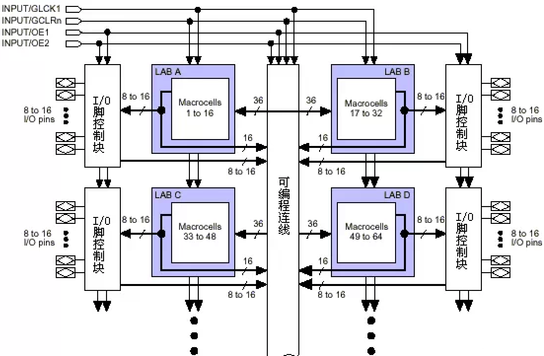
Figure 1 PLD internal structure based on product terms
This kind of PLD can be divided into three pieces of structure: Macrocell (Marocell), Programmable connection (PIA) and I/O control block. Macro unit is the basic structure of PLD, which realizes basic logic functions. The blue part in Figure 1 is a collection of multiple macrocells (because there are many macrocells, they are not drawn one by one). Programmable wiring is responsible for signal transmission and connects all macro units. The I/O control block is responsible for the electrical characteristics control of input and output, such as open collector output, slew rate control, three-state output and so on. The INPUT/GCLK1, INPUT/GCLRn, INPUT/OE1, INPUT/OE2 on the upper left of Figure 1 are global clocks, clearing and output enable signals. These signals have dedicated connections to each macro unit in the PLD. The delay of each macro unit is the same and the delay is the shortest.The specific structure of the macro unit is shown in the figure below:
![]() Figure 2 Macro unit structure
Figure 2 Macro unit structure
On the left is the product term array, which is actually an AND OR array. Each cross point is a programmable fuse. If it is turned on, it will realize the AND logic. The following product term selection matrix is an "or" array. The two complete the combinatorial logic together. On the right side of the figure is a programmable D flip-flop. Its clock and clear input can be programmed and selected. You can use dedicated global clear and global clock, or use the clock and clear generated by internal logic (product term array) . If you don't need a flip-flop, you can also bypass this flip-flop, and the signal is directly output to the PIA or output to the I/O pin.
The Logic Realization Principle of Product Term Structure PLD
Let's take a simple circuit as an example to explain in detail how PLD uses the above structure to implement logic. The circuit is as follows:![]() image 3Assuming that the output of the combinational logic (the output of AND3) is f, then f=(A+B)*C*(!D)=A*C*!D + B*C*!D (we denote D by !D "No")PLD will implement combinational logic f in the following way:
image 3Assuming that the output of the combinational logic (the output of AND3) is f, then f=(A+B)*C*(!D)=A*C*!D + B*C*!D (we denote D by !D "No")PLD will implement combinational logic f in the following way:![]()
Figure 4
A, B, C, D are input by the PLD chip's pins and then enter the programmable wiring array (PIA), there will be 8 A, A reverse, B, B reverse, C, C reverse, D, D reverse 8 Output. Each cross in the figure indicates connection (programmable fuse is on), so we get: f = f1 + f2 = (A*C*!D) + (B*C*!D). In this way, the combinational logic is realized. The realization of the D flip-flop in the circuit of Fig. 3 is relatively simple, directly using the programmable D flip-flop in the macrocell to realize. The clock signal CLK enters the global clock dedicated channel inside the chip after being input by the I/O pin, and is directly connected to the clock terminal of the programmable flip-flop. The output of the programmable flip-flop is connected to the I/O pin, and the result is output to the chip pin. In this way, the PLD completes the function of the circuit shown in Figure 3. (The above steps are all done automatically by the software, no human intervention is required)The circuit in Figure 3 is a very simple example, which can be completed with only one macrocell. But for a complex circuit, one macro unit cannot be realized. At this time, it is necessary to connect multiple macro units through parallel expansion items and shared expansion items. The output of the macro unit can also be connected to the programmable wiring array. It is the input of another macro unit. In this way, PLD can realize more complex logic.This product-based PLD is basically manufactured by EEPROM and Flash technology, and can work as soon as it is powered on, without the need for other chips to cooperate.
FPGA working principle and introduction
As mentioned earlier, FPGA is a product of further development on the basis of programmable devices such as PAL, GAL, EPLD, and CPLD. It emerged as a kind of semi-custom circuit in the ASIC field, which not only solves the deficiencies of custom circuits, but also overcomes the shortcomings of the limited gate circuits of the original programmable devices.
Because FPGA needs to be burned and written repeatedly, its basic structure for realizing combinational logic cannot be completed by a fixed NAND gate like ASIC, but can only adopt a structure that is easy to repeatedly configure. The look-up table can meet this requirement well. At present, mainstream FPGAs all use the look-up table structure based on SRAM technology, and some military and aerospace-grade FPGAs use the look-up table structure of Flash or fuse and anti-fuse technology. The method of changing the content of the look-up table by programming the file can realize the repeated configuration of the FPGA.
According to the basic knowledge of digital circuits, for an n- input logical operation, no matter it is an AND OR operation or an exclusive OR operation, there can only be 2n kinds of results at most. Therefore, if the corresponding result is stored in a storage unit in advance, it is equivalent to the realization of the function of the NAND gate circuit. The principle of FPGA is also the same. It configures the content of the lookup table by programming a file, thereby realizing different logic functions in the same circuit.
Look-up table (Look-Up-Table) is abbreviated as LUT, which is essentially a RAM. Currently, 4-input LUTs are mostly used in FPGAs, so each LUT can be regarded as a RAM with a 4-bit address line. After the user describes a logic circuit through the schematic diagram or HDL language, the PLD/FPGA development software will automatically calculate all possible results of the logic circuit, and write the truth table (ie the result) into RAM in advance, so that every signal is input Performing a logical operation is equivalent to inputting an address, looking up the table, finding out the content corresponding to the address, and outputting it.
An example of a 4-AND gate circuit is given below to illustrate the principle of LUT realization of logic functions.Example : Give a truth table that uses LUT to implement a 4-input AND gate circuit.
Table 1-1 The truth table of 4 input AND gate![]() It can be seen that the LUT has the same function as the logic circuit. In fact, LUT has faster execution speed and larger scale.
It can be seen that the LUT has the same function as the logic circuit. In fact, LUT has faster execution speed and larger scale.
Because LUT-based FPGA has a high degree of integration, its device density ranges from tens of thousands of gates to tens of millions of gates, and can complete extremely complex timing and logic combinational logic circuit functions, so it is suitable for high-speed, high-density high-end digital Logic circuit design field. Its components mainly include programmable input/output units, basic programmable logic units, embedded SRAM, rich wiring resources, underlying embedded functional units, embedded dedicated units, etc. The main design and manufacturers include Xilinx, Altera, Lattice, Companies such as Actel, Atmel, and QuickLogic, the largest of which are Xilinx, Altera, and Lattice.
As mentioned earlier, the FPGA is set up its working state by the RAM stored on the chip, so the on-chip RAM needs to be programmed during work. Users can adopt different programming methods according to different configuration modes. FPGA has the following configuration modes:
· Parallel mode: parallel PROM, Flash configuration FPGA;
· Master-slave mode: One PROM configures multiple FPGAs;
· Serial mode: Serial PROM configures FPGA;
· Peripheral mode: The FPGA is used as the peripheral of the microprocessor, and the microprocessor is programmed.
At present, the FPGAs produced by the two largest companies in the FPGA market, Xilinx and Altera, are all based on SRAM technology and need to be connected to an off-chip memory to save the program when in use. When powering on, FPGA reads the data in the external memory into the on-chip RAM, and after the configuration is completed, it enters the working state; after power off, the FPGA returns to a white chip and the internal logic disappears. In this way, the FPGA can not only be used repeatedly, but also does not need a special FPGA programmer, just a general EPROM, PROM programmer. Companies such as Actel and QuickLogic also provide FPGAs with anti-fuse technology, which can only be downloaded once. It has the advantages of radiation resistance, high and low temperature resistance, low power consumption and high speed. It is widely used in military and aerospace fields. FPGA cannot be repeatedly erased and written, it is more troublesome in the early development stage, and the cost is more expensive. Lattice is the inventor of ISP technology and has certain characteristics in small-scale PLD applications. Early Xilinx products generally do not involve military and aerospace-level markets, but there are already many products such as Q Pro-R that have entered this category.FPGA chip structureThe current mainstream FPGA is still based on look-up table technology, which has far exceeded the basic performance of the previous version, and integrates hard core (ASIC-type) modules with common functions (such as RAM, clock management, and DSP). As shown in Figure 1-1 (Note: Figure 1-1 is only a schematic diagram, in fact, each series of FPGA has its corresponding internal structure), FPGA chip is mainly completed by 6 parts, namely: programmable input and output unit , Basic programmable logic unit, complete clock management, embedded block RAM, abundant wiring resources, embedded low-level functional units and embedded dedicated hardware modules.![]()
Figure 1-1 The internal structure of the FPGA chip
The functions of each module are as follows:
1. Programmable input/output unit (IOB)
Programmable input/output unit is abbreviated as I/O unit, which is the interface part between the chip and the external circuit, and completes the driving and matching requirements of input/output signals under different electrical characteristics. The schematic structure is shown in the figure Shown in 1-2. The I/O in FPGA is classified by groups, and each group can independently support different I/O standards. Through the flexible configuration of the software, it can be adapted to different electrical standards and I/O physical characteristics, the size of the drive current can be adjusted, and the pull-up and pull-down resistances can be changed. At present, the frequency of I/O ports is getting higher and higher. Some high-end FPGAs can support data rates up to 2Gbps through DDR register technology.![]()
Figure 1-2 Schematic diagram of a typical IOB internal structure
The external input signal can be input to the inside of the FPGA through the storage unit of the IOB module, or directly input to the inside of the FPGA. When the external input signal is input into the FPGA through the storage unit of the IOB module, its hold time (Hold Time) requirement can be reduced, and it usually defaults to 0.
In order to facilitate management and adapt to multiple electrical standards, FPGA IOBs are divided into several banks (banks). The interface standard of each bank is determined by its interface voltage VCCO. A bank can only have one type of VCCO, but VCCOs of different banks can different. Only ports with the same electrical standard can be connected together, and the same VCCO voltage is the basic condition of the interface standard.
2. Configurable logic block (CLB)
CLB is the basic logic unit in FPGA. The actual number and characteristics of CLBs will vary from device to device, but each CLB contains a configurable switch matrix, which consists of 4 or 6 inputs, some selection circuits (multiplexers, etc.) and flip-flops composition. The switch matrix is highly flexible and can be configured to handle combinatorial logic, shift registers, or RAM. In Xilinx's FPGA devices, CLB is composed of multiple (generally 4 or 2) identical Slices and additional logic, as shown in Figure 1-3. Each CLB module can not only be used to implement combinational logic and sequential logic, but also can be configured as distributed RAM and distributed ROM.
![]()
Figure 1-3 Schematic diagram of a typical CLB structure
Slice is the basic logic unit defined by Xilinx. Its internal structure is shown in Figure 1-4. A slice is composed of two 4-input functions, carry logic, arithmetic logic, storage logic and function multiplexer. Arithmetic logic includes an exclusive OR gate (XORG) and a dedicated AND gate (MULTAND). An exclusive OR gate can enable a slice to implement a 2-bit full addition operation. The dedicated AND gate is used to improve the efficiency of the multiplier; the carry logic consists of a dedicated carry signal It is composed of a function multiplexer (MUXC) to implement fast arithmetic addition and subtraction operations; a 4-input function generator is used to implement a 4-input LUT, distributed RAM or 16-bit shift register (in the Slice of Virtex-5 series chips) The two input functions are 6 inputs, which can realize 6-input LUT or 64-bit shift register); the carry logic includes two fast carry chains to improve the processing speed of the CLB module.
![]()
Figure 1-4 Schematic diagram of a typical 4-input slice structure
3. Digital clock management module (DCM)
Most FPGAs in the industry provide digital clock management (all Xilinx FPGAs have this feature). Xilinx introduced the most advanced FPGA to provide digital clock management and phase loop lock. The phase loop lock can provide accurate clock synthesis, and can reduce jitter, and realize the filtering function.
4. Embedded block RAM (BRAM)
Most FPGAs have built-in block RAM, which greatly expands the scope and flexibility of FPGA applications. Block RAM can be configured as common storage structures such as single-port RAM, dual-port RAM, content address memory (CAM), and FIFO. RAM and FIFO are relatively popular concepts, so I won't repeat them here. The CAM memory has a comparison logic in each storage unit inside. The data written in the CAM will be compared with each internal data, and the address of all the data that is the same as the port data will be returned, so it is in the routed address. There are a wide range of applications in exchangers. In addition to block RAM, the LUT in the FPGA can also be flexibly configured into structures such as RAM, ROM, and FIFO. In practical applications, the amount of block RAM inside the chip is also an important factor in choosing a chip.
The capacity of a single block RAM is 18k bits, that is, the bit width is 18 bits and the depth is 1024. The bit width and depth can be changed as needed, but two principles must be met: First, the modified capacity (bit width depth) cannot be greater than 18k bits; secondly, the maximum bit width cannot exceed 36 bits. Of course, multiple pieces of block RAM can be cascaded to form a larger RAM. At this time, it is only limited by the number of block RAMs in the chip, and is no longer constrained by the above two principles.
5. Rich wiring resources
The wiring resource connects all the units inside the FPGA, and the length and craft of the connection determine the driving capability and transmission speed of the signal on the connection. There are abundant wiring resources inside the FPGA chip, which are divided into four different categories according to the process, length, width, and distribution location. The first category is global routing resources, which are used for the internal global clock and global reset/set routing of the chip; the second category is long-line resources, which are used to complete the routing of high-speed signals between chip banks and the second global clock signal; third Type is short-line resources, used to complete the logic interconnection and wiring between basic logic units; the fourth type is distributed wiring resources, used for proprietary clock, reset and other control signal lines.
In practice, the designer does not need to directly select wiring resources. The place and router can automatically select wiring resources to connect each module unit according to the topology and constraint conditions of the input logic netlist. Essentially, there is a close and direct relationship between the use of wiring resources and the result of the design.
6. The
embedded function module of the bottom layer mainly refers to the soft core (Soft Core) such as DLL (Delay Locked Loop), PLL (Phase Locked Loop), DSP and CPU. Nowadays, more and more abundant embedded functional units have made the single-chip FPGA a system-level design tool, enabling it to have the capability of software and hardware joint design, and gradually transition to the SOC platform.
DLL and PLL have similar functions. They can perform clock multiplication and division with high precision and low jitter, as well as duty cycle adjustment and shift equalization functions. The chip produced by Xilinx Company integrates DLL, the chip of Altera Company integrates PLL, and the new chip of Lattice Company integrates PLL and DLL at the same time. PLL and DLL can be conveniently managed and configured by tools generated by the IP core. The structure of the DLL is shown in Figure 1-5.
4. ![]()
Figure 1-5 Schematic diagram of a typical DLL module
5. 7. Embedded dedicated hard core The
embedded dedicated hard core is relative to the soft core embedded at the bottom. It refers to the hard core (Hard Core) with powerful FPGA processing capabilities, which is equivalent to ASIC circuits. In order to improve FPGA performance, chip manufacturers have integrated some dedicated hard cores inside the chip. For example: In order to improve the multiplication speed of FPGA, mainstream FPGAs have integrated dedicated multipliers; in order to adapt to communication bus and interface standards, many high-end FPGAs have integrated serial and parallel transceivers (SERDES), which can reach tens of Gbps. Sending and receiving speed.
Xilinx's high-end products not only integrate Power PC series CPUs, but also embed DSP Core modules. The corresponding system-level design tools are EDK and Platform Studio, and the concept of System on Chip (System on Chip) is proposed accordingly. Through PowerPC, Miroblaze, Picoblaze and other platforms, standard DSP processors and related applications can be developed to achieve the development goals of SOC. The concept of soft core, hard core and solid coreIP (Intelligent Property) core is a general term for integrated circuit cores with intellectual property cores. It is a repeatedly verified macro module with specific functions. It has nothing to do with the chip manufacturing process and can be transplanted to different semiconductor processes. At the SOC stage, IP core design has become an important task for ASIC circuit design companies and FPGA providers, as well as a manifestation of their strength. For FPGA development software, the more abundant IP cores it provides, the more convenient the user’s design and the higher its market occupancy. At present, the IP core has become the basic unit of system design and has been exchanged, transferred and sold as an independent design result.
In terms of the way in which IP cores are provided, they are usually divided into three categories: soft cores, hard cores, and solid cores. In terms of the cost to complete the IP core, the hard core is the most expensive; in terms of flexibility in use, the soft core has the highest reusability.
1. Soft
soft core means in EDA design before comprehensive register transfer level (RTL) model; middle finger particular FPGA design is hardware description language circuit, including logic description, netlist and help documentation. The soft core only undergoes functional simulation and needs to be synthesized and placed and routed before it can be used. Its advantages are high flexibility, strong portability, and allow users to configure themselves; the disadvantage is that the predictability of the module is low, there is a possibility of error in the subsequent design, and there is a certain design risk. Soft core is the most widely used form of IP core.
2. Solid core
solid nucleus refers in the EDA design netlist plane with planning information; in particular in the FPGA design can be seen with a soft core layout planning is usually provided in mixed form RTL code corresponding to the particular process and netlist . Combine the RTL description with the specific standard cell library for a comprehensive optimization design to form a gate-level netlist, which can then be used through layout tools. Compared with the soft core, the design flexibility of the solid core is slightly worse, but the reliability is greatly improved. At present, solid core is also one of the mainstream forms of IP core.
3. Hardcore
In the field of EDA design, the hard core refers to the verified design layout; in the FPGA design, it refers to the design with fixed layout and process and verified by the front-end and back-end, and the designer cannot modify it. There are two reasons why it cannot be modified: first, the system design has strict requirements on the timing of each module, and it is not allowed to disturb the existing physical layout; second, the requirement to protect intellectual property rights, and designers are not allowed to make any changes to it. The non-modification feature of IP hard core makes it difficult to reuse, so it can only be used in certain specific applications and has a narrow range of use.
